It’s common to see mask design in discussions about semiconductor manufacturing. This technique is key to making integrated circuits and other electronic parts. Custom wafer solutions have changed manufacturing. Now, achieving precise mask designs is easier than ever.
If you’re curious about how these solutions work and their significance in electronics, you’re in the right place!
Understanding Mask Design
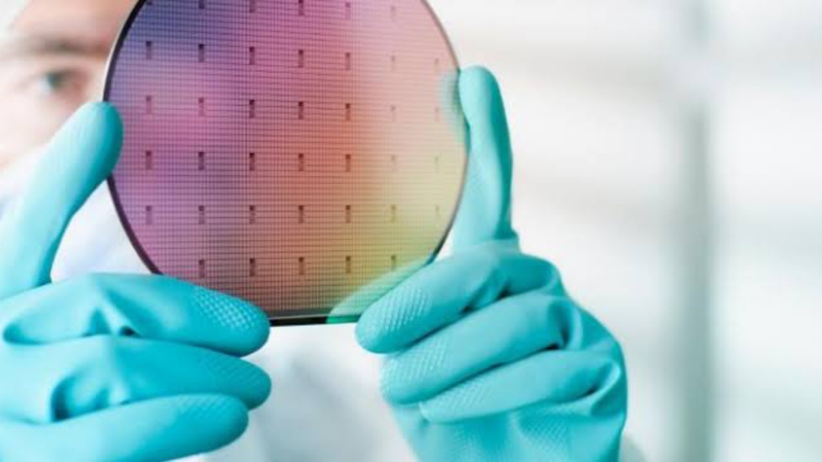
Mask design is a crucial part of producing chips for electronics. It refers to creating a mask, which is a pattern used to transfer designs onto a semiconductor wafer.
This pattern dictates where materials should be added or removed during the chip fabrication process. The ability to create intricate designs means that chips can be smaller, faster, and more efficient.
The importance of mask design lies in its ability to ensure each chip has the exact specifications needed for proper functioning. Poor mask designs raise the risk of mistakes. This can impact the whole production process.
The Role of Custom Wafer Solutions
Custom wafer solutions provide tailored services to meet specific needs in electronics manufacturing. They offer the flexibility to adapt to different mask design requirements.
Not all semiconductor projects are the same. Each one has unique needs based on its product requirements.
Companies use advanced technology and manufacturing methods to make customized wafers. These wafers can better accommodate unique mask designs. Custom solutions help engineers boost performance, making sure the wafers create high-quality chips.
Benefits of Custom Wafer Solutions
Numerous benefits come from using custom wafer solutions in mask design. Some of these advantages include:
Tailored Fit
Each semiconductor project has its unique set of performance, size, and functionality requirements. Custom wafer solutions ensure that mask designs are specifically tailored to meet these demands. This results in optimized layouts, improved yield, and higher functionality in end-use applications.
Enhanced Precision
The tech behind custom wafer solutions enables precise design and fabrication. This precision cuts down mistakes in line widths, layer alignment, and pattern integrity. So, it lowers the chance of defects and boosts chip quality consistency.
Speed of Production
Streamlined design workflows and flexible tooling allow for quicker development and turnaround times. Custom solutions speed up revisions. This allows mask designs to be changed or improved quickly. As a result, new products hit the market faster.
Cost Efficiency
Although custom wafer solutions may involve higher upfront investment, they offer long-term savings. Fewer production errors mean less waste and less rework. This also boosts manufacturing efficiency. Improved yields also reduce the per-unit cost of semiconductor chips.
Design Flexibility
Custom solutions handle various design challenges and technologies. These include advanced node geometries, 3D ICs, and mixed-signal or RF integration. This flexibility is crucial for pushing the boundaries of innovation and adapting to niche market demands.
Improved Reliability and Performance
Custom wafer solutions boost reliability, performance, and durability. They do this by aligning mask designs with specific electrical and thermal needs. This is especially important in critical fields like aerospace, automotive, and medical electronics.
IP Protection and Competitive Advantage
Custom mask designs protect intellectual property (IP). They create unique shapes that are tough to copy. This gives companies a competitive edge and safeguards proprietary circuit innovations.
The Process of Mask Design with Custom Wafer Solutions
The journey of creating a product begins with the idea of what you want to achieve. You can visualize how it will work in practice, especially when considering its electronic components. This involves designing the mask, which will guide how the wafer is processed.
Once the design is completed, it’s essential to produce patterned silicon wafers. This involves transferring the mask design onto the silicon wafer using lithography techniques.
The result is a wafer that has the patterns needed to create electronic circuits. Adopting custom wafer solutions at this stage significantly influences the quality and effectiveness of the resulting chips.
Advancements in Mask Design Technology
Technology continues to evolve, and recent advancements have had a profound impact on mask design. Improvements in software and fabrication techniques have enabled more complex designs.
Machine learning and artificial intelligence help improve mask design accuracy. These advanced technologies let engineers check designs. With AI, it’s possible to simulate how a mask design will behave, leading to better preliminary assessments and reliable results.
Applications of Custom Wafer Solutions
Custom wafer solutions with precise mask design are useful in many areas, not just consumer electronics. For instance, medical devices require top-notch precision and reliability. Chips used in these devices often rely heavily on custom mask designs to ensure they function correctly.
Also, the automotive industry is adopting custom mask designs for electronic parts in today’s vehicles. As cars become more technologically advanced, the need for sophisticated chips increases. Custom wafer solutions assist automotive engineers in crafting complex designs.
Challenges in Mask Design
Despite the numerous advantages of custom wafer solutions, some challenges come with achieving perfect mask design. Complexity is one significant hurdle. As designs get more intricate, they demand more time and resources to develop correctly.
Another challenge is the risk of errors during the transfer process. Even minor flaws in the mask design can lead to major issues later in production. Ensuring quality control is essential to mitigate these risks.
Future Trends in Mask Design
The future looks promising for mask design, especially with ongoing advancements in fabrication technology. Emerging techniques like extreme ultraviolet (EUV) lithography are set to redefine how masks are created and utilized in wafer production. EUV allows for more precise patterning, which can lead to better overall performance in chip manufacturing.
Moreover, as industries continue to push the boundaries of technology, the demand for custom solutions is expected to grow. New materials and processes will improve mask design. This change will also allow for more efficient production methods.
The Importance of Collaboration in Mask Design
Successful mask design relies heavily on collaboration among different stakeholders. Engineers, designers, and manufacturers must work together to achieve the desired outcomes. Open lines of communication ensure that everyone involved understands the requirements and constraints of the project.
Furthermore, partnerships with suppliers can lead to new insights and breakthroughs in mask design. Such collaborations can foster innovation and help overcome challenges that might hinder production capabilities.
Embracing the Future of Mask Design
In the rapidly evolving world of electronics, custom wafer solutions for mask design are more vital than ever. As technology advances, embracing innovative solutions becomes necessary for staying competitive. The future of mask design looks bright, and those who adapt will thrive in this exciting landscape.
Did you find this helpful? Don’t forget to visit our website and read more.